Thought leadership
Winning semiconductor FDI: The PITCH framework for investor-ready location propositions
Global semiconductor investment is becoming more diverse as the industry heads towards a $1tn market by 2030, driven by demand for artificial intelligence, advanced computing and electrification. Geopolitical tensions and talent shortages are prompting companies to rethink where they invest, with more capital flowing to new locations. For investment promotion agencies and economic development organisations, success will depend on understanding what investors want and communicating local strengths with clarity and focus.
-
Winning semiconductor FDI: The PITCH framework for investor-ready location propositions
-
Winning semiconductor FDI: The PITCH framework for investor-ready location propositions
-
Winning semiconductor FDI: The PITCH framework for investor-ready location propositions
-
Winning semiconductor FDI: The PITCH framework for investor-ready location propositions
- May 06, 2026
-
By Rory McRobbie
Global semiconductor investment has entered a new phase of expansion, competition and geographic diversification.
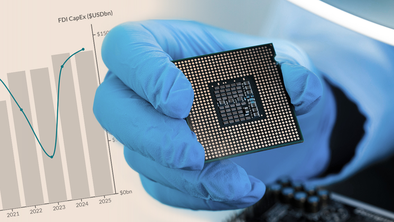
The industry is on track to become a $1tn market by 2030, driven by rising demand for artificial intelligence and advanced computing, data centre expansion, electrification and advanced manufacturing. According to fDi Markets, between 2021 and 2025, semiconductors attracted around $522bn in global greenfield FDI capital expenditure, making it the third-largest greenfield FDI sector globally after renewable energy and communications.
At the same time, location strategy is being fundamentally reshaped. Investment decisions are no longer driven by demand growth alone. Geopolitical fragmentation, supply-chain disruption, export controls and industrial policy are pushing semiconductor firms to reassess where they locate semiconductor facilities. For example, KPMG’s 2026 global semiconductor industry outlook found that 45% of semiconductor executives are actively increasing supply chain diversification of their supply chains. For investment promotion agencies (IPAs) and economic development organisations (EDOs), this creates a clear opportunity.
However, many locations still approach semiconductors as one broad sector, when investors evaluate a much more segmented set of fundamentally different activities within the semiconductor value chain. For example, R&D and design are driven by engineering talent, universities, research capability, digital infrastructure and innovation ecosystems. Wafer fabrication is capital-intensive, requiring multi-billion-dollar incentives, large industrial sites, advanced infrastructure, reliable power, water, wastewater capacity and deeply integrated supply chains. Assembly, testing and packaging can be a more accessible entry point for many locations, but still requires workforce scalability, operational reliability, and good logistics networks.
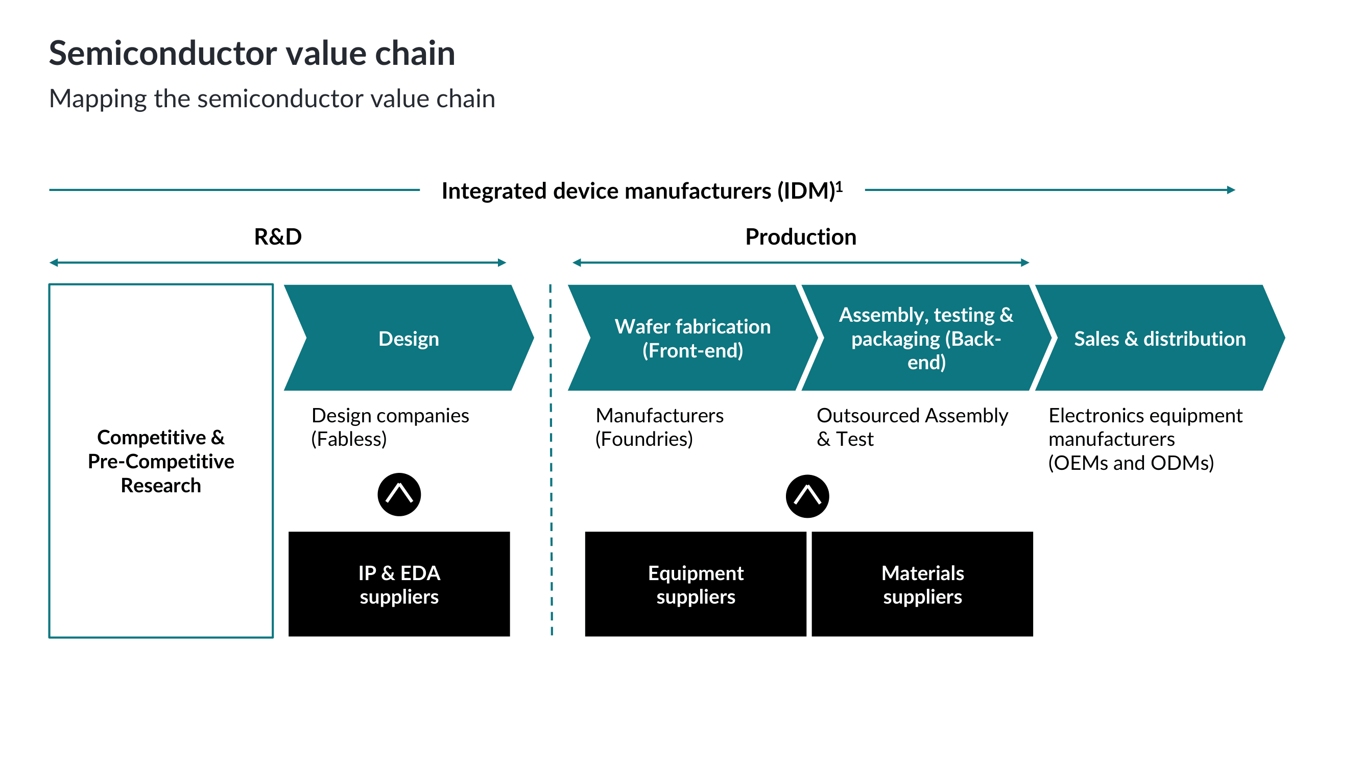
Note: IDMs are companies that span multiple or all stages of the value chain from design to manufacturing to assembly
That distinction matters because the geography of semiconductor FDI is not diversifying evenly. East Asia still accounts for as much as 75% of global semiconductor manufacturing capacity. Yet investment is increasingly flowing into new regions, particularly in more contestable segments of the value chain. According to the fDi Markets database between 2023 and 2025, India, Malaysia, Vietnam and Mexico collectively secured 27% of global semiconductor greenfield FDI projects, a significant increase from previous periods.
Talent is one of the main forces behind this shift. The semiconductor industry faces a global engineering shortage, with demand projected to outstrip supply by more than 100,000 professionals. As companies search for scalable engineering and technical talent, new locations are being pulled into the investment conversation.
The investor-readiness gap
Even when a location has credible assets, those assets are often poorly articulated for corporate decision-makers. Universities, industrial land, incentives, airports, technology parks and competitive costs only become persuasive when they are connected to the investor’s operating model.
That is why the quality of the pitch matters.
The strongest investment attraction propositions function as decision-support tools. They help a company answer the questions that determine whether a location moves from longlist to shortlist:
Can we build here?
Can we hire here?
Can we operate reliably?
Can suppliers support us?
Can state and local governments move at our speed?
Can this location support future phases of growth?
Arizona’s success in attracting Taiwan Semiconductor Manufacturing Company (TSMC) offers a useful proof point.
When TSMC selected Arizona for one of the most significant semiconductor investments in US history, the decision was not simply about land or incentives. It was about execution risk. TSMC needed a US location capable of supporting advanced semiconductor manufacturing at scale. That meant large industrial sites, reliable infrastructure, power, water planning, engineering talent, technician pipelines, supplier depth, public-sector coordination and long-term expansion capacity.
Arizona did not sell TSMC a site. It sold an operating platform.
For IPAs and EDOs, this is the shift now required. The strongest investor pitches have moved beyond the promotional storytelling often used at tech parks and trade shows. They now need to work as operating cases, showing how a location can support the investor from site selection through ramp-up and long-term expansion.
The following 5 key learnings show how investment promotion and economic development leaders can build semiconductor propositions relevant to investors’ interests
1. Start with the value chain, not the slogan
A location should not pitch “semiconductors” generically.
The first step is to define where the location is genuinely competitive across the value chain: R&D, design, materials, equipment, wafer fabrication, assembly, testing and packaging, or supplier operations. A location with strong universities and software talent may be better positioned for design or R&D than fabrication. A location with logistics assets, technical labour and proximity to electronics customers may be better suited for assembly, testing and packaging.
Semiconductor investments also rarely happen in isolation.
Companies want to see the foundations of a working supply chain, from research institutions and design houses to equipment suppliers, materials providers, testing facilities, logistics operators, cleanroom services and peer manufacturers. A strong ecosystem section should show anchor companies, suppliers, talent institutions, research assets, infrastructure and public-sector support.
Key learnings: Start with strategic focus. Show where your location fits in the semiconductor value chain and why that matters to the investor’s specific project. Use the ecosystem to prove momentum. Investors want to know they are joining a market with supplier depth, technical capability, exceedingly strong institutional support and room to grow.
2. Quantify the talent pipeline
Talent availability is one of the most important semiconductor location drivers.
An analysis of 200 global semiconductor FDI projects from fDi Markets between 2021 and 2025 shows that skilled workforce availability was cited in 43% of projects, ahead of technology and innovation, proximity to markets or customers, domestic market growth, industry clusters, and universities or research hubs.
High-performing pitches therefore move beyond broad claims about universities or workforce quality. They quantify the talent pipeline with engineering graduates, computer science talent, process engineers, cleanroom technicians, equipment maintenance skills, mechatronics programmes, apprenticeships and relevant employment in adjacent industries.
Investors need to see the workforce case clearly: who is available today, who is being trained for tomorrow, and how the pipeline can scale with the project.
Key learnings: Do not tell investors you have talent. Show them how the workforce engine works. A credible pitch connects existing skills, future graduates, training partners and ramp-up support into one clear hiring story.
3. Prove infrastructure readiness
For semiconductor manufacturing, infrastructure is not a supporting detail. It is often a deciding factor.
A serious pitch should address site availability, ownership, acreage, expansion potential, power capacity, water supply, wastewater, road access, airport connectivity, gas and chemical handling, construction labour, environmental approvals, permitting timelines and infrastructure funding.
This is especially important for locations that may face investor concerns around water, grid capacity or permitting risk. The answer is not to avoid these issues. It is to show a credible plan.
Key learnings: Infrastructure plays a major role in the location decision. Do not ask investors to trust that infrastructure will be solved later. Show what is ready now, what needs to be upgraded, who is responsible and when it can be delivered.
4. Demonstrate cost competitiveness
Many economic development presentations claim that a location is cost-competitive. Few can credibly prove it.
For semiconductor investors, cost comparisons should be specific and relevant. They may include engineering salaries, technician wages, construction costs, land costs, industrial utility costs, corporate taxes, property taxes, incentive value, housing affordability, cost of living and logistics costs.
The comparison set matters. A semiconductor investor may be comparing a location not only with neighbouring regions, but with Texas, Arizona, Ohio, Oregon, Singapore, Taiwan, South Korea, Japan or Malaysia.
Key learnings: Cost advantage only matters when it is credible. Benchmark labour, land, utilities, taxes, incentives and logistics against real competitor locations so investors can see where the business case improves
5. Explain incentives and regulatory pathways clearly
Semiconductor projects often depend on a complex mix of national incentives, regional tax benefits, infrastructure support, training grants, R&D incentives, property tax structures, customs benefits, permitting steps, environmental approvals and compliance requirements.
Investors need to understand which incentives apply, what they may be worth, what conditions are attached, when benefits are realised, what compliance is required and which agency manages the process. Incentives should be integrated into the broader business case, with enough detail to help companies assess value, timing, obligations and certainty.
Key learnings: Incentives only matter if investors can understand and access them. Show the potential value, the approval process, the obligations, the timeline and the support your organisation will provide.
The PITCH framework: from semiconductor ambition to investor confidence
The lesson from Arizona’s TSMC win is not that every location should chase a fabrication facility. It is that every location needs a sharper PITCH: a proposition that positions the location in the right part of the value chain, interprets investor requirements, translates data into a business case, coordinates delivery partners and helps the company scale over time.
For semiconductor investment attraction, the PITCH framework offers a simple test for whether a proposition is investor-ready.
P — Position your location in the value chain
Do not pitch semiconductors as one sector. Identify the specific part of the value chain where your location can credibly compete: R&D, design, materials, equipment, wafer fabrication, assembly, testing and packaging, supplier operations or headquarters functions.
I — Interpret the investor’s operating requirements
Build the pitch around the questions investors actually ask. Can we build? Can we hire? Can we operate reliably? Can suppliers support us? Can government move quickly? Can this location support future phases of growth?
T — Translate data into a decision-ready business case
Use evidence to make the location easier to compare. Quantify talent, benchmark costs, map the ecosystem, show infrastructure readiness and explain incentives in a way that supports the investor’s decision process.
C — Coordinate the partners needed to deliver
A high-performing pitch shows alignment. Government, utilities, education providers, workforce organisations, infrastructure agencies and local partners should be presented as part of a coordinated delivery system.
H — Help the investor land, scale and expand
The best pitches show phased entry scenarios, aftercare support, supplier development, workforce scaling and a long-term growth pathway. A strong semiconductor pitch builds confidence by connecting evidence, delivery partners, timelines and investor requirements into a clear operating case.
A new standard for semiconductor investment attraction
The semiconductor race is global, but the opportunity is unevenly distributed. Some locations will be credible for design. Others will have a stronger case for R&D, materials, equipment, advanced packaging or supplier operations. Only a small number will be able to compete for leading-edge wafer fabrication at scale.
That reality creates a new standard for IPAs and EDOs. Semiconductor attraction can no longer start with a broad sector ambition. It has to start with a clear view of where the location fits in the value chain, followed by a proposition that investors can test, compare and use.
The TSMC Arizona story shows what that standard looks like in practice. Arizona gave one of the world’s most important semiconductor companies credible answers to the questions that mattered most: could it build, hire, operate, source, move quickly and expand over decades?
That is the benchmark IPAs and EDOs now need to meet.
The next generation of semiconductor pitches will be judged by the clarity of their focus, the strength of their evidence and the credibility of their delivery plan. In a sector where projects can reshape regions for decades, the pitch is often the first test of whether a location understands the investor’s world.
How FT Locations can help
FT Locations, a specialised division of the Financial Times, is a global leader in corporate investment promotion strategy, working with national and subnational governments around the world to analyse and attract corporate investment. We specialise in transforming complex economic priorities into actionable investment attraction strategies backed by data, sector intelligence and global location benchmarks.
For EDOs and IPAs looking to attract semiconductor FDI, FT Locations can support with:
- Semiconductor value-chain opportunity assessment to identify whether your location is best positioned for R&D, design, materials, equipment, wafer fabrication, assembly, testing and packaging, supplier operations or headquarters functions.
- Sector-specific location benchmarking against competing global regions on talent, cost, infrastructure, incentives, ecosystem depth, market access and quality of life.
- Semiconductor value proposition development to translate local strengths into investor-ready messaging tailored to specific value-chain segments.
- Pitch deck and investor presentation development to help organisationsIPAs and EDOs move from broad promotion to evidence-led, decision-ready propositions.
- Sector marketing and content campaigns to position your location credibly with semiconductor executives, site selectors and corporate decision-makers.
- Investor targeting and lead generation intelligence using sector intelligence, fDi Markets data and corporate expansion signals to identify high-potential semiconductor investors.
- Ecosystem and supply-chain mapping to visualise anchor companies, suppliers, universities, research assets, infrastructure and public-sector partners.
- Investor outreach strategy and training to prepare teams for trade shows, missions, roadshows and direct corporate engagement.
- Aftercare and expansion strategy to help existing semiconductor and adjacent investors grow, deepen supplier relationships and create reinvestment opportunities.
Speak to our sales team today to see how we can help you
Further reading
Go beyond the headlines with the global database tracking greenfield investment
Strengthen your investment strategy with fDi Strategies
The semiconductor decade: A trillion-dollar industry
Global Semiconductor Industry Outlook for 2026
Strengthening the Global Semiconductor Supply Chain in an Uncertain Era
Learn more about FT Locations
FT Locations is the world's most comprehensive and trusted provider of investment promotion and economic development data and digital solutions for the foreign and domestic direct investment industry.
